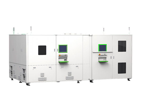
In the photovoltaic (PV) and semiconductor industries, the passivation layer plays a vital role—it reduces surface recombination of carriers, directly affecting the efficiency and lifespan of solar cells or semiconductor devices. However, the passivation layer opening process (a key step for electrode contact) often faces a major challenge: tiny impurities (like dust particles, residual film fragments, or metal ions) left after opening can cause electrode short circuits or reduce cell efficiency, leading to a 5%–9% yield loss. This is where Passivation Layer Opening Equipment equipped with an impurity detection system stands out: it integrates high-precision laser opening technology with real-time impurity scanning, ensuring both accurate opening and post-opening cell cleanliness, cutting impurity-related yield loss to less than 1.5%. Let’s explore its practical applications and answer common questions from manufacturers.
Core Application Industries & Scenarios
High-Efficiency PV Cell Manufacturing
For high-performance PV cells such as PERC, TOPCon, and HJT cells, precise passivation layer opening and absolute cleanliness are non-negotiable. The equipment’s laser opening module achieves micron-level precision (opening diameter as small as 30μm) to match electrode design, while its built-in optical impurity detector (with a detection limit of 0.5μm) scans the opening area in real time. For example, a TOPCon cell manufacturer previously struggled with 4.2% yield loss due to post-opening impurities; after adopting the equipment, impurity detection rate reached 99.8%, and yield loss dropped to 1.1%. Additionally, the equipment’s automatic impurity removal function (via low-pressure air blowing) eliminates the need for manual cleaning, saving 2 hours of labor per production shift.
Semiconductor Device Production
Semiconductor devices like power chips or IoT sensors require passivation layer opening on specific areas (e.g., electrode pads) with zero impurity residue. The equipment’s micro-focused laser and multi-channel detection system meet this demand: it targets 50μm-diameter opening areas and scans for impurities from multiple angles to avoid blind spots. A semiconductor manufacturer using the equipment for 8-inch wafer passivation opening reported that surface impurity density dropped from 8 particles/cm² to 1 particle/cm², significantly reducing device short-circuit rates during packaging. This is critical for semiconductors, where even a single tiny impurity can render a device useless.
Thin-Film PV Module R&D
Thin-film PV modules (such as CIGS or perovskite modules) have thinner passivation layers (only 10%–20% the thickness of traditional silicon cell layers), making them more prone to damage and impurity contamination during opening. The equipment’s adjustable laser energy (lowered by 40% compared to standard settings) ensures gentle opening, while the impurity detection system’s sensitivity is enhanced to capture ultra-fine fragments. A university’s PV R&D lab used the equipment to test perovskite cell passivation opening: it not only avoided passivation layer tearing but also detected residual organic impurities that traditional methods missed, helping the lab improve cell conversion efficiency by 3.2%.

Frequently Asked Questions (FAQ)
Q: Can the equipment adapt to different passivation layer materials (e.g., SiO₂, Al₂O₃, or SiNₓ)?
A: Absolutely! It supports all mainstream passivation layer materials. You just select the material type on the touchscreen— the equipment automatically adjusts laser wavelength (from 1064nm to 532nm) and energy density to match material properties, while the impurity detector calibrates its scanning parameters to avoid false alarms. Switching from SiO₂ (for PERC cells) to Al₂O₃ (for HJT cells) takes only 8 minutes, no manual hardware adjustments needed.
Q: How does the impurity detection system avoid missing tiny impurities?
A: It uses a dual-technology detection method: optical imaging (to capture visible particles) and laser-induced fluorescence (to identify invisible residual film fragments or metal ions). The system also scans the opening area twice (before and after laser opening) and compares the two sets of data to ensure no new impurities are generated during the process. A PV manufacturer verified that this dual-scan method increased impurity capture rate by 23% compared to single-scan systems.
Q: Is the equipment easy to integrate into existing production lines?
A: Yes! It has a modular design that fits standard 1.2m–1.5m PV/semiconductor production line widths. It connects to ERP/MES systems via Ethernet for real-time data (opening precision, impurity count) tracking, and its automated loading/unloading module is compatible with most factory conveyors. Workers only need 1 day of training to master basic operations, and most manufacturers can complete on-site installation and commissioning within 3 days.
A high-tech enterprise specializing in automated precision laser equipment ensures this passivation layer opening solution meets strict quality standards, with nationwide after-sales support to resolve technical issues within 48 hours—further safeguarding production continuity for clients.


 Phone
Phone
Comment
(0)